System Upgrade on Tue, May 28th, 2024 at 2am (EDT)
Existing users will be able to log into the site and access content. However, E-commerce and registration of new users may not be available for up to 12 hours.For online purchase, please visit us again. Contact us at customercare@wspc.com for any enquiries.
"This book is more suited for researchers already familiar with WBS who are interested in developing new WBG materials and devices since it provides the latest developments in new materials and processes and trends for WBS and UWBS technology."
IEEE Electrical Insulation Magazine
With the dawn of Gallium Oxide (Ga2O₃) and Aluminum Gallium Nitride (AlGaN) electronics and the commercialization of Gallium Nitride (GaN) and Silicon Carbide (SiC) based devices, the field of wide bandgap materials and electronics has never been more vibrant and exciting than it is now. Wide bandgap semiconductors have had a strong presence in the research and development arena for many years. Recently, the increasing demand for high efficiency power electronics and high speed communication electronics, together with the maturity of the synthesis and fabrication of wide bandgap semicon-ductors, has catapulted wide bandgap electronics and optoelectronics into the mainstream.
Wide bandgap semiconductors exhibit excellent material properties, which can potentially enable power device operation at higher efficiency, higher temperatures, voltages, and higher switching speeds than current Si technology. This edited volume will serve as a useful reference for researchers in this field — newcomers and experienced alike.
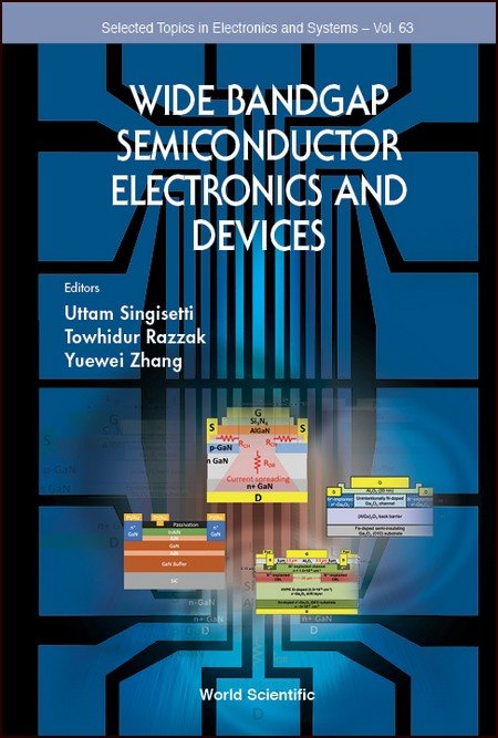
This book discusses a broad range of topics including fundamental transport studies, growth of high-quality films, advanced materials characterization, device modeling, high frequency, high voltage electronic devices and optical devices written by the experts in their respective fields. They also span the whole spectrum of wide bandgap materials including AlGaN, Ga2O₃and diamond.
Sample Chapter(s)
Preface
Substrate Effects in GaN-on-Silicon RF Device Technology
Contents:
- Preface
- Substrate Effects in GaN-on-Silicon RF Device Technology (H Chandrasekar)
- Gallium Oxide Field Effect Transistors — Establishing New Frontiers of Power Switching and Radiation-Hard Electronics (M H Wong and M Higashiwaki)
- High Efficiency AlN/GaN HEMTs for Q-Band Applications with an Improved Thermal Dissipation (R Kabouche, R Pecheux, K Harrouche, E Okada, F Medjdoub, J Derluyn, S Degroote, M Germain, F Gucmann, C Middleton, J W Pomeroy and M Kuball)
- Recent Progress in Gallium Oxide and Diamond Based High Power and High-Frequency Electronics (M N Hasan, E Swinnich and J-H Seo)
- Application of Atom Probe Tomography for Advancing GaN Based Technology (O G Licata and B Mazumder)
- β-(Al,Ga)₂O₃ for High Power Applications — A Review on Material Growth and Device Fabrication (Z Jian, K Khan and E Ahmadi)
- Opportunities and Challenges in MOCVD of β-Ga₂O₃ for Power Electronic Devices (M A Mastro, J K Hite, C R Eddy, Jr , M J Tadjer, S J Pearton, F Ren and J Kim)
- Theory of High Field Transport in β-Ga₂O₃ (K Ghosh and U Singisetti)
- Ultra-Wide Bandgap AlxGa₁-ₓN Channel Transistors (T Razzak, S Rajan and A Armstrong)
- On the Progress Made in GaN Vertical Device Technology (D Ji and S Chowdhury)
- Modeling and Simulation of Quasi-Ballistic III-Nitride Transistors for RF and Digital Applications (K Li and S Rakhejar)
- Recent Progress in III-Nitride Tunnel Junction-Based Optoelectronics (Z Jamal-Eddine, Y Zhang and S Rajan)
Readership: Engineers and research scientists working on High-Speed Electronics.