Microstructure of electronic-grade polycrystalline silicon core-matrix interface
Abstract
This paper focuses on the problems encountered in the production process of electronic-grade polycrystalline silicon. It points out that the characterization of electronic-grade polycrystalline silicon is mainly concentrated at the macroscopic scale, with relatively less research at the mesoscopic and microscopic scales. Therefore, we utilize the method of physical polishing to obtain polysilicon characterization samples and then the paper utilizes metallographic microscopy, scanning electron microscopy-electron backscatter diffraction technology, and aberration-corrected transmission electron microscopy technology to observe and characterize the interface region between silicon core and matrix in the deposition process of electronic-grade polycrystalline silicon, providing a full-scale characterization of the interface morphology, grain structure, and orientation distribution from macro to micro. Finally, the paper illustrates the current uncertainties regarding polycrystalline silicon.
1. Introduction
Polycrystalline silicon, as the fundamental material for the electronic and photovoltaic industries, has found widespread applications in artificial intelligence, automatic control, information processing, and photovoltaic power generation, earning it the moniker “the cornerstone of the microelectronics edifice”. With the impetus from the photovoltaic and integrated circuit industries, the apparent demand for polycrystalline silicon has witnessed a continuous upsurge in recent years. Electronic-grade polycrystalline silicon, characterized by high purity and low impurity, has emerged as a pivotal direction for the advancement of China’s semiconductor industry. It is extensively used in the production of solar photovoltaic panels (6N-9N) and integrated circuits (9N-11N), representing the purest material attainable through human industrialization.1,2,3 With the rapid development of electronic components, the demand for electronic-grade polycrystalline silicon is on the rise, necessitating the manufacturing industry to enhance the purity, uniformity, and yield of electronic-grade polycrystalline silicon.
As the research technology for electronic-grade polycrystalline silicon continues to progress, the preparation process and material performance have undergone significant enhancements. Various preparation methods such as the Czochralski method, Zone melting method, and Magnetic-field which applied Czochralski method have been widely applied.4,5,6 Furthermore, the indicators of electronic-grade polycrystalline silicon, including the number of crystal defects and the equivalent oxygen content, have undergone substantial improvements.7 The demands for purity and uniformity in electronic-grade polycrystalline silicon are notably high. During the production process, conductive carbon, as one of the primary impurities in semiconductor materials, exerts a severe impact on the electrical performance of the products, leading to a reduction in the breakdown voltage of silicon devices and posing significant harm to high-power thyristor devices. Additionally, the high concentration of carbon in polycrystalline silicon can promote the formation of oxygen precipitation, which, in turn, induces secondary defects such as dislocations and stacking faults, resulting in an increase in leakage current of silicon devices and a reduction in the yield.7,8 Moreover, the joint interaction of carbon and oxygen complicates the impact of impurities on the material and device performance, leading to a shortened service life.9 The uneven chemical element distribution and the distribution of crystal morphology and corresponding resistivity in polycrystalline silicon significantly affect the quality stability of polycrystalline silicon. The unevenness in the composition and structure exerts a substantial impact on the quality stability of polycrystalline silicon. The distribution of chemical elements and the corresponding resistivity in polycrystalline silicon crystals is also uneven. The resistivity values are highest in the bottom nucleation zone, irregular grain growth, columnar grain growth, irregular grain growth, and the presence of straight resistivity contour lines.9,10,11
The structure at the interface between the silicon core and the matrix plays a crucial role in determining the final microstructure and performance of polycrystalline silicon. The nucleation process of polycrystalline silicon can be explained by two primary mechanisms: inheritance nucleation and heterogeneous nucleation. Inheritance nucleation refers to the formation of new polycrystalline silicon particles on the surface of single-crystal silicon or already formed polycrystalline silicon particles. Heterogeneous nucleation, on the other hand, refers to the formation of polycrystalline silicon particles on the surface of impurities or other foreign substances present in the silicon solution.12 After nucleation, polycrystalline silicon grains grow within the matrix and form an interface with the matrix. The structure and properties of the interface directly impact the size, orientation, and defects of polycrystalline silicon grains.10,13,14,15 However, the specific structure of electronic-grade polycrystalline silicon and the matrix interface is not yet fully understood. Therefore, this study, employing advanced microstructure characterization instruments such as metallographic microscope, scanning electron microscope combined with backscattered electron diffraction technology (SEM-EBSD), and aberration-corrected scanning transmission electron microscope (AC-STEM), aims to achieve a full-size characterization of the microstructure and composition of the silicon core–matrix interface, to reveal the transition layer structure in the early deposition growth area of electronic-grade polycrystalline silicon, and to provide better theoretical support and guidance for the preparation and application of electronic-grade polycrystalline silicon.
2. Results and Discussions
2.1. Electronic-grade polysilicon characterization sample preparation
In this paper, we used the 8-inch electronic-grade polysilicon provided by the New Energy Branch of the Huanghe Hydropower Development Co., Ltd. Using diamond wire cutting, three blocks were cut out in the axial direction, named 1.1, 1.2, 1.3, 2.1, 2.2, 2.3, and so on. The 1.1/2.1 samples contain a silicon core and a matrix to meet the requirements for the observation and characterization of the interface transition layer between the silicon core and the matrix.
The preparation of polysilicon metallographic samples is completed by physical methods, and the specific operation process is shown in Fig. 1. The surface of the prepared metallographic sample should be very smooth and mirror-like. Especially for samples containing the interface between the silicon core and the matrix, the boundary could be directly visible on the surface to facilitate the extraction of subsequent samples.
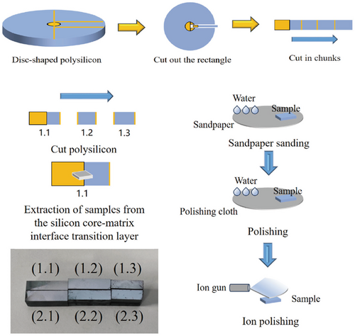
Fig. 1. Schematic diagram of intercepting 8-inch polycrystalline silicon rod and sample extraction of the silicon core–matrix interface; Schematic diagram of the metallographic sample preparation process.
2.2. Macroscale characterization and analysis via metallurgical microscope
The metallographic microscopy image of the silicon core indicates an overall single-crystal structure, with a relatively smooth and uniform surface morphology. However, there are certain undulations present on the sample’s surface, as depicted by the fine-line features in Figs. 2(a) and 2(b), indicating the presence of twins in the structure. Additionally, the appearance of triangular pits in Fig. 2(c) suggests the convergence of triple-junction boundaries, resulting in stress concentration and significant surface undulations on the silicon core. Figures 2(a)–2(c) suggest that the structure of the silicon core should be a uniform single crystal, which bodes well for subsequent large-scale epitaxial growth. However, the presence of twinning indicates that the growth of the silicon core has adopted a preferential direction, leading to the generation of stress from the core, ultimately reducing its strength and electrical performance. While twinning can to some extent enhance its strength, the widespread and multi-layered occurrence of twinning under the requirement for a single-crystal silicon core limits the further deposition growth of polycrystalline silicon.
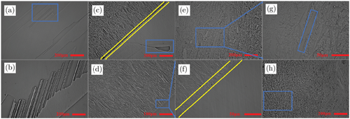
Fig. 2. Metallographic micrograph of polysilicon from core to matrix.
The interface between the silicon core and the matrix exerts a significant influence on the epitaxial growth and electrical performance of polycrystalline silicon. Figures 2(c), 2(d), and 2(f) reveal the presence of a single crystal structure at the silicon core, while the matrix exhibits a polycrystalline structure. The formation of the amorphous region from single crystal to polycrystalline at the interface places limitations on the further epitaxial growth of silicon, leading to a drastic deterioration in its electrical performance.
It is obvious that the irregularities occur at the interface between the silicon core and the matrix in Figs. 2(c) and 2(f). Growing polycrystalline silicon matrix by single core deposition can be size-free and ideally have relatively regular amorphous interfaces because there are the fewest defects and the lowest energy barrier. The irregularity of the interface is due to the degree of single crystal of the silicon core, and the preparation process leads to more defects such as layer faults at the interface, and it is accompanied by the improvement of the energy barrier. This will affect the matrix of the deposited growth is not uniform enough, resulting in ordered structures such as twins, columnar crystals, and nanocrystals. When the interface irregularity is large, some pores will be generated in the amorphous region, and the enrichment of impurity elements will occur, which will affect the electrical and mechanical properties of polysilicon and limit its industrial production and application.
The larger-view analysis of the matrix, as depicted in Figs. 2(e), 2(g), and 2(h), reveals a polycrystalline structure rich in nano twinning regions and extensive columnar crystals. While the large accumulation of twinning in the region adversely impacts the performance of the matrix due to the preferential orientation growth, the formation of small and numerous nano twinned regions to some extent contributes to strengthening the mechanical strength of polycrystalline silicon. However, the interlacing twinning often leads to stress concentration, resulting in decreased strength. Furthermore, the presence of columnar crystals in Fig. 2(g) leads to a further decline in the electrical performance of polycrystalline silicon, although it can enhance the mechanical strength, offering some benefits in industrial manufacturing. Yet, the adverse impact of the columnar crystal region on the electrical performance is more pronounced. The occurrence of various types of grains is one of the reasons why polycrystalline silicon cannot grow on a large scale. The irregularity of the transition layer at the silicon core–matrix interface is a significant factor in the appearance of small, numerous nano twinned and columnar crystal regions in the matrix. On one hand, due to the irregularity of the interface itself, the twinning structure of the silicon core may continue to extend outward, resulting in the manifestation of small, numerous twinned regions due to the polycrystalline growth characteristics of the matrix. On the other hand, despite the fact that the amorphous region at the interface has already isolated the majority of the single-crystal structure of the silicon core, the energy barrier at the interface itself leads to a certain orientation in the polycrystalline growth of the matrix, which is another reason for the enrichment of nano twinned regions in the matrix. For the growth of polycrystalline silicon, subsequent efforts should focus on eliminating the nano twinned regions to a more reasonable extent. The ideal situation is to completely remove nano twinned regions and maintain a highly pure polycrystalline form of the matrix.
In summary, the large-scale polycrystalline silicon is composed of the silicon core, the amorphous interface, and the polycrystalline silicon matrix. The amorphous region and the silicon core are particularly crucial for the epitaxial growth of the polycrystalline silicon matrix, especially the relevant structural form at the interface, which directly affects whether the polycrystalline silicon can successfully achieve large-scale growth and the consistency of its electrical performance.
3. Microscale Characterization and Analysis via SEM-EBSD
3.1. Silicon core
Figures 3(a)–3(d) demonstrate that the silicon core exhibits a single-crystal structure, with a relatively consistent orientation, and the grain size is predominantly concentrated at 1500m and above, essentially constituting a large-sized single-crystal structure. However, it is evident that twinning occurs in the 60∘ direction, which compromises the mechanical strength and electrical performance of the silicon core. As depicted in Figs. 3(b) and 3(d), although twinning can to some extent reinforce the silicon core, its presence is detrimental to the electrical performance of the polycrystalline silicon. Figure 3(b) directly confirms the extensive presence of twinning with a 60∘ orientation difference in the silicon core, resulting in the intersection of twinning in multiple directions, leading to stress concentration, reduced strength, susceptibility to breakdown, compromised performance, and constraints on further epitaxial growth. The appearance of extensive orientation differences in the grain and grain boundary is consistent with the observed twinning structure results under the metallographic microscope.
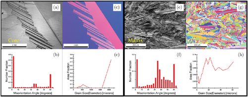
Fig. 3. EBSD diagram of the silicon core and matrix.
Figures 3(e)–3(h) indicate that the matrix of polycrystalline silicon comprises extensive polycrystalline regions, with the presence of some twinning and oriented grains such as columnar crystals. The orientation and size distribution of the grains in Figs. 3(f) and 3(h) also confirm the presence of oriented grains, as the randomness of the polycrystalline regions in the matrix is significantly lower compared to the amorphous region at the silicon core–matrix interface. This is manifested in larger grain sizes and an uneven distribution of orientations. The reduction in the randomness of the polycrystalline regions directly leads to the deterioration of electrical performance, resulting in reduced breakdown voltage and limitations in application. Furthermore, the presence of various grain regions leads to an increase in defects, which is detrimental to the large-scale epitaxial growth of polycrystalline silicon.
3.2. Silicon core–matrix interface
Figures 4(a) and 4(c) demonstrate that the amorphous arrangement of the interface is more irregular. In particular, some amorphous regions at the interface have a certain orientation, which makes the silicon epitaxial growth have a certain selection direction, and finally grows into ordered crystal regions such as twins and columnar crystals. This reduces the randomness of the polycrystalline region and hinders its large-scale growth. The extension of the single crystal silicon core and the tendency for further extension at the interface lead to the irregularity of the amorphous region.
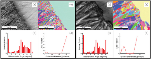
Fig. 4. EBSD diagram of the silicon core–matrix interface.
Figures 4(b) and 4(d), as well as Figs. 3(b), 3(d), 3(f), and 3(h) illustrate that the orientation difference between the two sides of the interface is increasing. The transition from the single crystal and twinning structure of the silicon core to the amorphous interface, and then to the polycrystalline matrix results in the random orientation of the matrix grains. However, compared to the multiple orientations at the amorphous interface, the growth of the matrix has a relatively preferred direction, as evidenced by the nonrandomness of the matrix grain orientation in Fig. 4. This is a consequence of the irregularity at the interface.
Figures 4(e)–4(h) confirm the irregularity of the amorphous transition layer. When the matrix extends outward, there is a probability that the structure of the silicon core will continue to extend outward, reducing the polycrystalline behavior of the matrix. At high magnifications, the interface is predominantly amorphous region with relatively random orientation. However, the randomness of the grain orientation and size distribution is reduced compared to what is observed at low magnifications, indicating a decrease in the randomness of the polycrystalline silicon random distribution. This phenomenon reflects the irregularity of the amorphous region and its impact on the random distribution of the matrix polycrystalline zones during the extension growth. In particular, when the orientation of the silicon core is consistent, the ordered arrangement outward will be lower, resulting in a more ordered arrangement of the amorphous region and thus affecting the random distribution of the matrix.
In conclusion, the SEM-EBSD maps from low to high magnifications provide further and deeper evidence for information drawn from the previous metallographic microscope results. In particular, the existence of the amorphous region at the silicon core–matrix interface and the irregularity of the amorphous region interface have been confirmed. Furthermore, the occurrence of twinning and columnar crystals in the matrix has also been validated. This series of work has important guiding significance for the production and preparation of polycrystalline silicon. Furthermore, the relevant analysis of the interface zone directly indicates the factors that limit the large-scale epitaxial growth of polycrystalline silicon in the production process and the factors leading to the decrease in electrical performance after epitaxy. This has important guiding significance for directing the production of polycrystalline silicon in the industry.
4. Nanoscale Characterization and Analysis via STEM
Figures 5(a) and 5(b) indicate that the silicon core is a single crystal structure, while a twinning structure is present in the core, as shown in Figs. 5(c)–5(f). Particularly, the multi-directional twinning intersection structure is observed in Fig. 5(e), which confirms the existence of the multi-directional twinning structure previously observed at the macroscopic and mesoscopic scales in metallography and SEM-EBSD. This significantly limits the electrical performance and mechanical strength of the silicon core, and affects the deposition and growth structure of the interface and matrix. Similarly, in Figs. 5(c) and 5(d), it can be observed that the twinning structure of the silicon core can directly extend over the interface, confirming the behavior of twinning structure of the silicon core crossing the interface for growth, directly impacting the structure of the interface and matrix in the deposition of polycrystalline silicon.
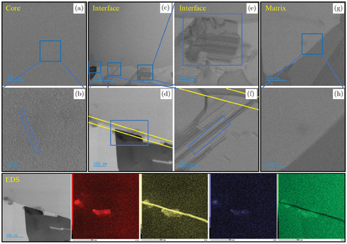
Fig. 5. HADDF images of the silicon core, interface, and matrix.
Figures 5(c)–5(f) demonstrate that the interface of the polycrystalline silicon core–matrix is irregular, directly confirming the irregularity observed in metallography and SEM-EBSD in the previous text, and the STEM-EDS mappings at the interface demonstrate the enrichment of carbon, oxygen, and boron elements at the interface. The uneven composition and enrichment of impurity phases at the interface may be one of the most important reasons for limiting the generation of large-sized polycrystalline silicon. STEM-EDS images demonstrate that oxygen is almost entirely enriched at the interface, greatly affecting the purity of the deposition and growth of polycrystalline silicon. Figures 5(d) and 5(f) indicate that the interface is amorphous region with the enrichment of impurity elements, leading to certain stress and deposition barriers at the interface, which is also one of the reasons for limiting the large-scale epitaxial growth of polycrystalline silicon. Figures 5(g) and 5(h) intuitively reflect the microstructure of the polycrystalline silicon matrix as a polycrystalline structure and a relatively uniform distribution, with no observed enrichment of other elements in the STEM-EDS.
Figure 5 illustrates the microstructure of the polycrystalline silicon from the core outward: the silicon core is composed of single crystal and twinning; the interface is made up of amorphous regions enriched with oxygen elements; and the matrix consists of irregular polycrystalline. The transitional layer structure at the interface plays a crucial restrictive role in the large-scale epitaxial growth of polycrystalline silicon. As previously mentioned, the irregularity of the interface and the randomness of the amorphous distribution can lead to the formation of ordered grains in the epitaxial polycrystalline silicon matrix, greatly affecting the electrical performance and strength of polycrystalline silicon, limiting its widespread industrial application.
5. Conclusion
This study provides a thorough study of the core–matrix interface during the deposition growth of large-sized polycrystalline silicon. Multiple characterizations from macroscopic to microscopic and then to nanoscales were performed to reveal that the amorphous interface between the silicon core and the epitaxial matrix is the key factor limiting the large-sized epitaxial growth in polycrystalline silicon.
The results of metallurgical microscopy and EBSD showed that the interface of polysilicon had a significant effect on the deposition and growth of the matrix. It is manifested that the transition region at the interface is not regular, and the grains in the transition zone from single crystal silicon core to polycrystalline matrix show high disorder and energy barrier.
The results of AC-TEM directly prove the irregularity of the interface, the occurrence of higher disorder of grains, and higher energy barrier behavior in the transition region. At the same time, the interface is enriched with light impurity elements, oxygen, carbon, as well as boron. The silicon core exhibits a single-crystal structure, while the matrix presents a polycrystalline structure. The amorphous nature of the interface, the irregularity in grain orientations of the matrix close to the interface, and the enrichment of impurity elements concurrently lead to the occurrence of structural faults and energy barriers at the interface, which is highly detrimental to the growth of the polycrystalline matrix. This result provides certain guiding significance to the production of polycrystalline silicon.
With the continuous emergence of new technologies, the application prospects of electronic-grade polycrystalline silicon will be broader. The application of electronic-grade polycrystalline silicon in the fields of optoelectronic devices, biomedicine, and other areas will gradually expand. The demand for electronic-grade polycrystalline silicon in the field of solar cells will also continue to increase. Low-cost, high-output, and high-efficiency preparation processes is the future development trend, making it increasingly important to characterize the finer structure and composition of polycrystalline silicon.
Acknowledgments
The work was completed with the support of the unveiling project of “Application Research on Carbon and Other Trace Impurities and Microstructure Characterization Technology on the Surface of Electronic Grade Polysilicon” by Qinghai Xince Technology Co., Ltd. of the Huanghe Hydropower Development Co., Ltd., project number: XCKJ-FY (2024) No. 1 (total No. 25).
ORCID
Bochen Lu  https://orcid.org/0009-0007-5934-4691
Yuxuan Yang  https://orcid.org/0009-0008-3700-612X
Yang Zhang  https://orcid.org/0000-0002-7543-0502
Rong Qin  https://orcid.org/0009-0008-0808-5201
Xinlu Xue  https://orcid.org/0009-0000-7222-1310
Jinyue Peng  https://orcid.org/0009-0001-4986-3486
Haijun Wu  https://orcid.org/0000-0002-7303-379X


