Microstructure evolution from silicon core to surface in electronic-grade polycrystalline silicon
Abstract
Large-size electronic-grade polycrystalline silicon is an important material in the semiconductor industry with broad application prospects. However, electronic-grade polycrystalline silicon has extremely high requirements for production technology and currently faces challenges such as carbon impurity breakdown, microstructure and composition nonuniformity and a lack of methods for preparing large-size mirror-like polycrystalline silicon samples. This paper innovatively uses physical methods such as wire cutting, mechanical grinding and ion thinning polishing to prepare large-size polycrystalline silicon samples that are clean, smooth, free from wear and have clear crystal defects. The material was characterized at both macroscopic and microscopic levels using metallographic microscopy, scanning electron microscopy (SEM) with backscattered electron diffraction (EBSD) techniques and scanning transmission electron microscopy (STEM). The crystal structure changes from single crystal silicon core to the surface of the bulk in the large-size polycrystalline silicon samples were revealed, providing a technical basis for optimizing and improving production processes.
1. Introduction
Polycrystalline silicon, as the basic material for the electronics and photovoltaic industries, is widely used in fields such as artificial intelligence, automatic control, information processing and solar power generation.1 It is known as the “cornerstone of microelectronics.” Due to the growth in the photovoltaic and integrated circuit industries, the apparent demand for polycrystalline silicon in China has been continuously increasing in recent years.2
Polycrystalline silicon can be classified into two categories based on purity: solar grade (6N–9N) and electronic grade (9N–11N). Electronic-grade polycrystalline silicon is one of the purest substances obtained in human industry.3 Currently, there is a significant gap in the supply of electronic-grade polycrystalline silicon.
However, the production of electronic-grade polycrystalline silicon requires extremely high technical standards and faces the following challenges.1,4 Carbon is a major impurity in semiconductor materials that can significantly impact electrical performance, particularly in silicon devices.5 It can induce breakdown voltage and pose a risk to high-power thyristor devices. High concentrations of carbon in polycrystalline silicon promote the formation of oxygen precipitates. The combined effects of carbon and oxygen complicate the influence of impurities on material and device performance, resulting in a shortened lifespan.6 Additionally, the nonuniform microstructure and composition of polycrystalline silicon can greatly affect its quality stability.7 These issues are influenced by process parameters and techniques during production.5 These two challenges greatly hinder the large-scale production of electronic-grade polycrystalline silicon with a diameter of 12 in or above. The technical bottlenecks in the electronic-grade polycrystalline silicon industry may further impact downstream semiconductor companies and chip manufacturing.
Currently, there is a lack of specific characterization of the structure of polycrystalline silicon at the micro level in production research. Therefore, based on the challenges aforementioned, it is urgent for us to utilize advanced microstructure characterization technologies to study the morphology, structural composition and crystal structure on the surface of polycrystalline silicon materials, providing technical guidance for controlling carbon content in the production process of polycrystalline silicon.
Currently, the characterization of polycrystalline silicon samples focuses mainly on macroscopic and mesoscopic scales, and there is rare characterization of large polycrystalline silicon blocks.8 The preparation of large-sized polycrystalline silicon characterization samples mostly relies on chemical methods, which can cause damage to the surface morphology formed a suede structure. This limits the ability to observe different structures on a single sample. Due to the lack of mature large-size polysilicon surface treatment technology, the analysis and characterization of polysilicon are mainly limited to local and small-size nanoscale microstructure. For example, Maulid et al.9 conducted a study of dislocation patterns common in the tops of industrial directionally solidified polycrystalline silicon castings. However, for the production and preparation of large-size polysilicon, there is still a lack of comprehensive characterization of the microstructure evolution from the silicon core to the surface. The lack of comprehensive characterization of the microstructure evolution from the silicon core to the surface limits the technical improvement and perfection of the preparation of large size polysilicon, and further affects its transportation and popularization.
To solve the limitations of the above technology, this paper innovatively uses physical method combined with plasma polishing to prepare large mirror samples for the characterization of optical microscope, scanning electron microscopy (SEM) and backscattered electron diffraction (EBSD). Compared with chemical methods samples prepared by physical methods have no surface damage and can reflect their intrinsic structural characteristics to the greatest extent.10 In addition, Wire-cut and plasma polishing is also used in this paper. Wire-cut has the advantages of high precision and no deformation during processing. Plasma polishing compared with chemical polishing has high polishing precision, no sub-surface damage, suitable for various sizes and profiles, environmental protection and pollution-free. Therefore, this paper innovatively uses pure physical method to prepare large-sized polycrystalline silicon metallographic specular samples, enabling nondestructive observation of surface structures and completion of macro-to-mesoscale to microstructure observations of large-sized samples.
In response to the production characterization challenges faced by the polycrystalline silicon production industry, an innovative approach utilizing block cutting, mechanical grinding and polishing, as well as ion polishing, was employed to complete the preparation of large-scale microscopic samples. Combined with multi-scale structural characterization techniques, this method yielded a wide range of grain characteristics of polycrystalline silicon from its core to its surface, thus supplementing the research on the preparation of smooth surfaces of polycrystalline silicon and the characterization of related large-scale samples. This provides a technical basis for the optimization and improvement of production processes.
2. Sample Preparation and Characterization Methods
2.1. Metallographic sample preparation
As shown in Fig. 1, the large 12-in polycrystalline silicon block (the silicon core size is ) is cut into three long strip-shaped blocks measuring from the core towards the outer side using wire cutting, and their orientations are marked. Manual grinding is performed on a rotating disc using silicon dioxide paper with sequentially decreasing particle sizes of 800–4000 grit. During the grinding process, it is important to apply balanced force until the scratches appear neat and uniform under an optical microscope. Finally, polishing is performed using silicon dioxide polishing suspension (0.05m) to achieve a matte finish. Subsequently, the sample is thoroughly cleaned by ultrasonication in anhydrous ethanol and acetone to remove any residual hydrocarbons on the polished surface.
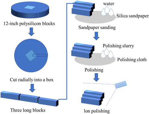
Fig. 1. Schematic diagram showing metallographic sample preparation of 8-in polycrystalline silicon rod.
Finally, the polished samples are subjected to surface ion thinning using an ion thinning instrument.11 The power is set between 3kV and 6kV, the tilt angle is set between 10∘ and 20∘, and the duration is set between 15min and 30min. After the ion thinning process, the samples can meet the requirements for full-scale observation from the macroscopic to mesoscopic to microscopic levels.
2.2. Material characterization methods
To investigate the morphological, dimensional and orientational variations of the grains in different regions of large polycrystalline silicon blocks, we initially employed an optical microscope to observe the structural changes from the silicon core to the outer surface of the polished samples. Subsequently, we conducted microscopic observation and orientation characterization of the material using a scanning electron microscope (SEM) equipped with electron backscatter diffraction (EBSD) and a scanning transmission electron microscopy (STEM).
Electron backscatter diffraction (EBSD) is a technique that utilizes diffracted electron beams to obtain crystallographic information about the sample. By analyzing the orientation structure information carried by the backscattered electrons, we can acquire comprehensive insights into grain boundaries, phases, grain orientations, textures and strains within the sample. Focused ion beam (FIB) is a technology that utilizes ion beams for processing and analysis. It is based on controlling the energy and focus of the ion beam and can precisely etch, cut, deposit or implant the material. FIB typically uses high-energy ion beams, such as argon ions or radium ions, which are focused to very small diameters by a focusing device, allowing for high-resolution processing and analysis. The FIB has the advantages of high precision, high resolution and noncontact. FIBs are widely used in various fields. In the semiconductor industry, it is used for tasks such as chip repair, circuit modification and sample preparation. In the field of materials science and nanotechnology, FIB can be used to prepare nanodevices, etch nanostructures and characterize samples. In this paper, high-quality samples for TEM characterization were obtained by FIB. STEM is a technique used in the field of electron microscopy to study the structure and composition of materials at the atomic scale. In this paper, the required data were obtained by using the FIB of Thermo Scientific Helios 5ux equipped with EBSD, with an electron beam operating voltage of 5kV and an ion beam operating voltage of 30kV. In STEM, a focused electron beam is scanned across the sample, and the transmitted electrons are collected and used to form an image. This allows for high-resolution imaging of the sample, providing valuable information about its structure and properties. In this paper, the required data were obtained by using STEM model JEM-ARM300F2 with an operating voltage of 300kV.
3. Results and Discussion
3.1. Metallurgical microscope characterization from core to surface of polycrystalline silicon
3.1.1. Silicon core
Figures 2(a1) and 2(a2) reveal the characteristics of the microstructure of the silicon core. Overall, the silicon core exhibits a typical single-crystal structure, with a smooth and even surface and no presence of minor dendrites. The interior of the single-crystal silicon core displays abundant subgrain structures. In Figs. 2(a1) and 2(a2), we can clearly observe blocky subgrains, mostly in square or rectangular shapes, with smooth and neat edges, relatively clean interiors and a low defect rate. Further observation in Figs. 2(b1) and 2(b2) reveals interconnected elongated twins with consistent orientation, with grain widths ranging from 30m to 100m and exhibiting smooth and sharp boundaries.
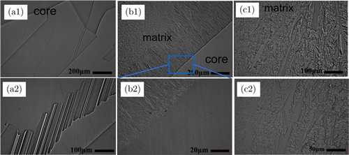
Fig. 2. Metallographic micrograph of a polycrystalline silicon matrix: (a1) and (a2) the core of polycrystalline silicon; (b1) and (b2) the interface of polycrystalline silicon; (c1) and (c2) the matrix of polycrystalline silicon.
Large-sized silicon wafers consist of single-crystal silicon with abundant subgrain structures. In the epitaxial growth of polycrystalline silicon, the single-crystal silicon core serves as the starting point for the formation of polycrystalline silicon, guiding and controlling crystal growth on a large scale. Subgrains, as small-scale ordered structures within the crystal, typically contain lattice defects and dislocations. The local symmetry breaking caused by the defects in silicon core can introduce novel phenomena, that is, increasing electron scattering, reducing electron mobility within the crystal and thereby negatively impacting conductivity.9 Furthermore, the defects such as twins, stacking faults and dislocations contained within subgrains may lead to localized stress accumulation, which, in turn, can cause differential grain nucleation and growth on the surface of polycrystalline silicon due to stress concentration.
3.1.2. Interface between the core and matrix
As shown in Fig. 2(b), a clear interface is evident between the silicon core and the matrix of the material, with an amorphous region at the interface. The emergence of the amorphous region is attributed to the discontinuity between different crystal structures and the mismatch in atomic arrangements.12 At the interface between single-crystal and polycrystalline regions, atomic diffusion may occur under the influence of temperature or stress. Such diffusion can lead to structural disorder and the formation of amorphous regions. The presence of amorphous interfaces typically introduces electron scattering, restricts carrier mobility, leads to electron–hole recombination and subsequently affects carrier lifetime, ultimately resulting in decreased conductivity.13 The presence of amorphous interfaces also affects the band structure of polycrystalline silicon, potentially leading to the formation of additional charge states near the interface, consequently influencing electron band filling and migration.
The silicon core exhibits a smooth single-crystal structure with no apparent defects. In contrast, the matrix is composed of polycrystalline structures, with the area adjacent to the interface being a region of small grain nucleation.14 In the vicinity of the nucleation area, approximately 400m thick dendritic columnar crystals are observed, extending outward perpendicular to the interface, presenting a significant contrast with other areas of the matrix. The formation of the columnar crystals may be attributed to the large temperature gradient in the interface region, resulting in a high cooling rate that favors preferred grain orientation, thereby forming an orderly arrangement of columnar crystals.
Conversely, the regions of the matrix far from the interface exhibit a radiating crystalline structure with no specific orientation, with grain sizes around 10–20m. The formation of the radiating crystal structure is due to the high solidification rate at lower temperatures in this region, leading to rapid nucleation and growth.15 Anisotropic radiative grains have larger grain boundary area than columnar grains, which means that their scattering effect on charge carriers is also increased. The smaller the grain size, the lower the strength of the material. This may also be one of the reasons for the production of silicon powder during transportation.
3.1.3. Matrix
As illustrated in Fig. 2(c), the polycrystalline silicon in the matrix is predominantly comprised of a high-density elongated grain structure, exhibiting dendritic grains growing radially, indicating a specific orientation of the polycrystalline silicon during its growth process. In addition to the elongated grains in the matrix region, there are numerous elongated twins displaying a certain orientation along the radial direction. The presence of twins indicates localized stress concentration during the material’s growth process, with rapid grain growth in stress concentration zones resulting in larger twins compared to the elongated grains in the matrix.15 Furthermore, the emergence of twins introduces irregularities in the crystal structure. Acting as electron scattering centers, twins affect the free transmission of electrons, resulting in a reduction in the average free path length of electrons and thereby impacting the conductivity. Additionally, twins can serve as initiation points for cracks, leading to crack propagation and increased material brittleness. The abundance of twins and the increased brittleness caused by stress concentration make the material prone to silicon powder generation during transportation, affecting the promotion of large-sized polycrystalline silicon for solar panel applications.
With the aid of metallographic microscopy, we have gained a preliminary understanding of the grain morphology and evolution of polycrystalline silicon wafers from the core to the surface. The complexity of the internal structure of polycrystalline silicon underscores the importance of a comprehensive understanding of its microstructural features. Further analysis and confirmation work are imperative to fully comprehend these structural characteristics. A more in-depth and precise exploration of grain orientation and size variations necessitates the assistance of advanced characterization techniques such as SEM-EBSD. This will aid in revealing more microscopic structural details, providing a deeper scientific basis for the performance and application of the silicon core.
3.2. SEM-EBSD characterization from core to surface of polycrystalline silicon
3.2.1. Silicon core
As depicted in Figs. 3(a) and 3(b), the SEM and EBSD images illustrate the internal structure of the large polycrystalline silicon core. Throughout this process, we observe an increase in the number and length of elongated, strip-shaped features from the core to the edge region, gradually coalescing into large subgrains. The edge region predominantly exhibits large subgrains, with a higher abundance. The boundaries of the large subgrains are characterized by a multitude of stacking faults and dislocation defects, the accumulation of which results in structural nonuniformity at the boundaries. Furthermore, the junctions of multiple subgrains can lead to issues of stress concentration.
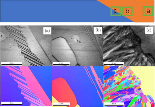
Fig. 3. SEM-EBSD plot of the polysilicon: (a), (b) Abundant twins and subgrains in silicon core; (c) interface between the single-crystal core and polycrystalline matrix within the large-sized polycrystalline silicon.
The crystal defects present on the surface of the single-crystal silicon block, serving as the starting point for polycrystalline silicon epitaxial growth, such as lattice defects and dislocations, may propagate during the growth process of polycrystalline silicon, leading to defects in the polycrystalline silicon product and thereby affecting its crystalline quality.16 These findings hold significant importance for the manufacturing and quality control of polycrystalline silicon products, providing robust support for a deeper understanding of the internal structure and properties of polycrystalline silicon.
3.2.2. Interface between the core and matrix
As shown in Fig. 3(c), the SEM and EBSD images depict the interface between the single crystal and polycrystalline matrix within the large-sized polycrystalline silicon block. Clear observations from Fig. 3(b) reveal the abundant presence of twinning structures on the surface of the silicon core, alongside indications of curvature issues at the interface, suggesting insufficient surface flatness of the single-crystal silicon. This inadequacy may stem from the low surface flatness of the single-crystal silicon and the accumulation of surface defects, negatively impacting the continuity of the lattice during epitaxial growth, thereby affecting the quality of the epitaxial wafer.
Regarding the epitaxial growth matrix, the grain boundaries at the interface appear in a fine state, with sizes in the range of a few micrometers and lacking distinct orientation, forming a region of small grain nucleation. These grains gradually elongate in areas distant from the interface, forming larger columnar crystals with clear orientation extending outward perpendicular to the interface. From the EBSD image in Fig. 3(c), it is evident that the columnar crystals near the unevenness of the single-crystal silicon surface exhibit a distinctly different orientation from other regions. This inconsistency in orientation may be attributed to differing interface orientations, potentially causing stress concentration issues at the polycrystalline silicon interface.
In conclusion, the surface flatness and interface orientation issues of the single-crystal silicon may have a negative impact on the continuity of the lattice and the crystal quality during epitaxial growth.17 Therefore, it is imperative to take measures to improve the surface flatness of the single-crystal silicon, reduce the accumulation of surface defects and adjust the epitaxial growth conditions to enhance the orientation of the grains at the interface, mitigate the inconsistent growth direction of the columnar crystals, and thereby alleviate the effects of stress concentration.
3.2.3. Matrix
As depicted in Fig. 4, the SEM and EBSD images vividly illustrate the evolution of the internal structure of polycrystalline silicon, gradually moving away from the silicon core, from region (a) to region (d). In Figs. 4(a1)–4(a4), the vicinity of the interface exhibits the gradual reduction and termination of large columnar grain crystals, forming a divergent, chrysanthemum-like grain morphology. The grain sizes primarily range between 20m and 60m, exhibiting low-angle specific orientation. Notably, there are numerous micrometer-sized small grains present in the interstices between the grains, serving as a cushion to mitigate stress concentration issues when different-oriented large grain crystals come into contact. Overall, the matrix near the single crystal core predominantly exhibits a chrysanthemum-like grain structure, with micrometer-sized small grains filling the gaps.
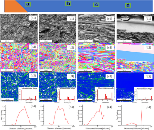
Fig. 4. SEM-EBSD plot at the boundary of the polysilicon matrix. (a1) and (a2) Columnar grain crystals and chrysanthemum-like grain morphology at the vicinity of the interface; (b1) and (b2) small grains with random orientation and grains with certain orientations in the midsection of the polycrystalline region; (c1) and (c2) columnar crystal structure in the tail end of the polycrystalline region; (d1) and (d2) Twins in edge of the polycrystalline region.
Figure 4(b) presents the image of the midsection of the polycrystalline region, where the grains significantly grow, exhibiting a radial-specific orientation. The presence of micrometer-sized small grains in the gaps notably decreases. In Figs. 4(c) and 4(d), compared to regions (a) and (b), the grains in region c further move away from the silicon core, exhibiting more significant elongation and enlargement. These grains demonstrate a distinct orientation along the radial direction, densely arranged with a pronounced columnar crystal structure. Meanwhile, there are still numerous small grains with random orientation present in the interstices between the grains.
Moreover, consistent with the optical microscopy data, midsection twinning appears along the radial direction, with a width of approximately 100m. The appearance of twinning in the end part of the material indicates localized stress concentration during the epitaxial growth process of the polycrystalline silicon. This may be related to the lack of stress relief due to the differing epitaxial growth orientations caused by the initial surface nonuniformity of the single-crystal silicon. As the grains grow, internal stresses increase, thereby promoting the growth of twinning.
While the elongated small grains effectively increase the grain boundaries, thereby impeding the movement of dislocations and slip, thus enhancing the strength and hardness of the polycrystalline silicon, it is important to note that grain boundaries act as scattering centers for electrons, influencing the free transmission of electrons. This reduces the average free path length of electrons, ultimately impacting the conductivity of the polycrystalline silicon. Therefore, a careful balance between grain boundaries and conductivity needs to be considered in the design of polycrystalline silicon to meet the performance requirements of specific application areas.
3.3. STEM characterization from core to surface of polycrystalline silicon
The STEM images presented in Figs. 5(a1) and 5(a2) depict the interface between a large-sized polycrystalline silicon (poly-Si) silicon core and the matrix. An uneven boundary is observed at the connection between the epitaxial matrix and the silicon core. The silicon core appears smooth overall, with no distinct features. At the epitaxial matrix, rich twinning, dislocation and subgrain features are evident.
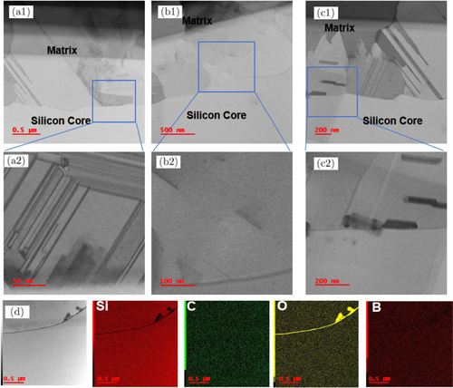
Fig. 5. STEM and EDS plots at the Interface of the polysilicon: (a1) and (a2) Abundant twinning in epitaxial matrix; (b1) and (b2) dislocations and lattice distortions in epitaxial matrix; (c1) and (c2) large-angle subgrains in silicon core; (d) EDS mapping at the interface.
As shown in Figs. 5(a1)–5(a2) at higher magnification, the interior of the subgrains reveals abundant twinning. Most twinning ceases at the subgrain boundaries. The formation of twinning may be a response to external strain or heat treatment to adapt to the external environment or reduce internal strain. Unlike the internal structure of a single twin, the atomic arrangement at the twin boundaries of twinning with different orientations involve dislocations and lattice distortions to overcome the lattice mismatch between adjacent twins, maintaining overall structural stability, as shown in Figs. 5(b1) and 5(b2).18 Similarly, at the subgrain boundaries, there are numerous stacking faults and dislocation defects that typically increase electron scattering, reducing the electron mobility in the crystal and thus negatively impacting conductivity. The intersection of subgrain boundaries and twin junctions may lead to the accumulation of local stress, and the stress concentration on the surface of polycrystalline silicon further results in differential nucleation and growth of epitaxial polycrystalline silicon grains.
In Figs. 5(c1) and 5(c2), evident large-angle subgrains can be observed, likely associated with stresses during the polycrystalline silicon formation process. The interior of the subgrains contains a small amount of twinning. While the interface between twinning and the epitaxial polycrystalline matrix is smooth, it is clearly observable that subgrain boundaries extend across the interface into the polycrystalline matrix. This is attributed to the orientation of the matrix significantly influencing the formation and properties of epitaxial polycrystalline silicon. If the lattice structure and orientation of the matrix exhibit orientational ordering in a certain direction, epitaxial polycrystalline growth tends to favor grains with the same orientation on the matrix. This orientational ordering aids in the formation of an ordered polycrystalline structure. When the matrix lattice matches well with the epitaxial polycrystalline lattice, stress and distortion are minimized, contributing to the improvement of the quality of the polycrystalline film.19 Figures 5(c1) and 5(c2) reveal the impact of the disordered single crystal matrix on the orientation of epitaxial polycrystalline at the nanoscale.
The STEM-EDS mappings at the interface demonstrate the enrichment of oxygen at the interface in Figs. 5(d1) and 5(d2). The uneven composition and enrichment of impurity phases at the interface may be one of the most important reasons for limiting the generation of large-sized polycrystalline silicon. This oxygen-rich assembly leads to adverse effects on the electrical properties of the junction, including increased resistance, changes in barrier shape and increased impurity trapping centers.20 In order to reduce the adverse effects of oxygen enrichment on electrical properties, some methods can be used, such as optimizing growth conditions, controlling oxygen content and interfacial reaction, to reduce the degree of oxygen enrichment and improve electrical properties. In the process of polysilicon manufacturing, controlling the degree of oxygen enrichment at the junction is one of the important factors to improve the device performance.
3.4. Summary and analysis of large-sized polysilicon topography
In summary, our investigation uncovers that the central silicon core in large wafers is primarily single crystal silicon with intricate sub-grain structures. Moving toward the surface, larger polygonal sub-grains gradually replace smaller ribbon-like sub-grains, resulting in noticeable twin boundaries. There is obvious oxygen enrichment at the interface of silicon core and epitaxial matrix. The polycrystalline silicon matrix expands outward from the starting point of epitaxial growth, evolving through zones like a small grain nucleation area, a columnar crystal zone, a diverging chrysanthemum-shaped crystal zone and a coarse columnar crystal composite twin crystal zone.
Surface irregularities and nonuniform structures caused by twinning negatively affect lattice continuity during epitaxial growth, impacting the quality of the resulting polycrystalline silicon. Abundant grain boundaries and large twin crystals in the polycrystalline silicon act as scattering centers, reducing electrical conductivity. The widespread twin crystal structure and stress concentration serve as a starting point for crack initiation, propagating cracks and increasing material brittleness. Numerous twin crystals and heightened material brittleness due to stress make the material prone to generating silicon powder during transportation, affecting long-distance transport of large-sized polycrystalline silicon. The junction between polysilicon core and epitaxial matrix is mainly caused by oxygen impurity during grain growth, grain boundary energy difference and interface reaction, which leads to adverse effects on the electrical properties of the junction, including the increase of resistance, the change of barrier shape and the increase of impurity trapping center.
4. Conclusions
The large-scale electronic-grade polycrystalline silicon is an important material in the semiconductor industry with promising prospects. With the rapid development of information technology, the demand for semiconductor products continues to increase and electronic-grade polycrystalline silicon, as a crucial component of semiconductor materials, will continue to be in high demand. The innovative use of physical methods such as wire cutting, mechanical grinding and ion thinning polishing in the preparation of large-sized polycrystalline silicon samples with clean, smooth surfaces, no wear and clear crystal defects is documented in this paper. The material was characterized from macroscopic to microscopic levels using metallographic microscopy, electron backscatter diffraction and SEM technique. We have used advanced characterization techniques, such as STEM, for more detailed microscopic structural details.
Our investigation uncovers that the central silicon core in large wafers is primarily single crystal silicon with intricate subgrain structures. Moving towards the surface, larger polygonal subgrains gradually replace smaller ribbon-like subgrains, resulting in noticeable twin boundaries. There is an obvious oxygen enrichment at the interface of silicon core and epitaxial matrix. The polycrystalline silicon matrix expands outward from the starting point of epitaxial growth, evolving through zones like a small grain nucleation area, a columnar crystal zone, a diverging chrysanthemum-shaped crystal zone and a coarse columnar crystal composite twin crystal zone. The findings reveal the crystal structure changes of the large-sized polycrystalline silicon samples from the single-crystal silicon core to the matrix surface, providing a technical basis for optimizing and improving production processes.
In this paper, we have provided a preliminary understanding of grain morphology and evolution but better emphasize the need for further analysis and confirmation. This will aid in revealing more microscopic structural details, providing a deeper scientific basis for the performance and application of large-scale polycrystalline silicon.
Acknowledgments
The authors would like to acknowledge the financial support from the unveiling project by Qinghai Xince Technology Co., Ltd., Huanghe Hydropower Development Co., Ltd., Project No. XCKJ-FY (2024) No. 1 (total No. 25). The authors would also like to thank the strong support from the Instrumental Analysis Center of Xi’an Jiaotong University. Jinyue Peng and Yuxuan Yang authors contributed equally to this work.
ORCID
Jinyue Peng  https://orcid.org/0009-0001-4986-3486
Yuxuan Yang  https://orcid.org/0009-0008-3700-612X
Yang Zhang  https://orcid.org/0000-0002-7543-0502
Xinlu Xue  https://orcid.org/0009-0000-7222-1310
Bochen Lu  https://orcid.org/0009-0007-5934-4691
Rong Qin  https://orcid.org/0009-0008-0808-5201
Haijun Wu  https://orcid.org/0000-0002-7303-379X


